 Turnkey PCB Design & Fabrication for High-Performance Systems
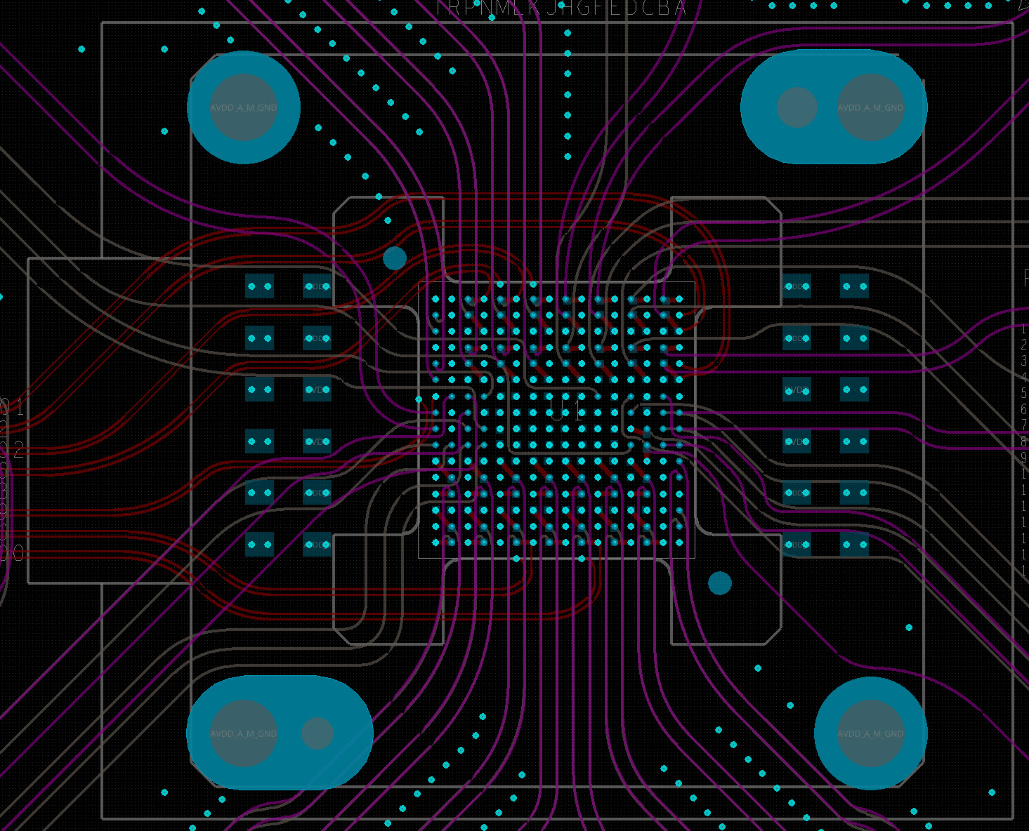
At Wild River Technology, we offer turnkey PCB design and fabrication solutions, managing every stage from schematic capture and library development to layout, fabrication oversight, and final delivery. With a proven track record supporting complex, high-speed designs under tight deadlines, we bring unmatched technical depth, speed, and precision to every project.
Our design process focuses on cost-efficiency, performance, and reliability, continuously evolving to meet the demands of today’s most advanced electronics applications.
End-to-End Project Management
Every PCB project at WRT is guided by an experienced team that ensures transparency, precision, and collaboration. Our project management includes:
- Direct supervision and primary point-of-contact for the board design engineer
- Ongoing design checks as each section is completed
- Placement and post-layout design reviews with the customer
- Weekly progress reports to keep your team aligned
PCB Design & Fabrication Services
At Wild River Technology, we offer turnkey PCB design and fabrication solutions, managing every stage from schematic capture and library development to layout, fabrication oversight, and final delivery. With a proven track record supporting complex, high-speed designs under tight deadlines, we bring unmatched technical depth, speed, and precision to every project.
Our design process focuses on cost-efficiency, performance, and reliability, continuously evolving to meet the demands of today’s most advanced electronics applications.
End-to-End Project Management
Every PCB project at WRT is guided by an experienced team that ensures transparency, precision, and collaboration. Our project management includes:
- Direct supervision and primary point-of-contact for the board design engineer
- Ongoing design checks as each section is completed
- Placement and post-layout design reviews with the customer
- Weekly progress reports to keep your team aligned
Pre-Design Activities
- Define team structure and responsibilities
- Set up a shared collaboration folder (e.g., Dropbox)
- Review project goals, functional requirements, data rates, and signal integrity needs
- Identify timing constraints, signal integrity challenges, and design trade-offs
- Review initial PCB placement (Visio mockup or customer-provided concept)
- Establish project schedule, milestones, and risk mitigation strategies
PCB Design Phase
- Coordinate symbol and footprint library creation
- Define and apply design rules and timing constraints
- Conduct placement reviews and iterative feedback loops
- Route standard and high-speed nets with critical signal integrity considerations
- Perform balance routing and constraint checks
- Final design reviews and QA
- Generate and deliver a complete fabrication package
