
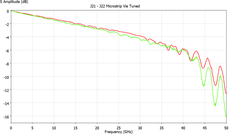
 WRT has a highly proprietary material ID methodology, using a host of structures that are used to fit material ID in X-Y and Z PCB orientation. There is both a model-based pre-fabrication and measure-based post-verification phase built into each program. Our material Identification and modeling is EDA-centric, fitting the models in 3D electromagnetic (EM) simulation software.
Construction of a reduced size Channel Modeling Platform (CMP) that focuses solely on material ID is core to this activity. There is a partial set of verification structures that are used to verify the models.
In the post-fabrication phase, measurements of the CMP undergo comprehensive S-parameter quality checks which proceeds careful calibration. Cross-sectional analysis using a PCB test strip included with each CMP is also done, as well as PCB fabrication verification.
Measurements, comprehensive model material ID fit reports, PCB libraries of the CMP, and measurement to simulation examples are included in each final report.
The Material Identification program is a an investment in the front end of the project, early in the design state. Our systematic methodology yields scores of benefits
- Modeling using Ansys HFSS (3D), Cadence Clarity
- 3D X-Y and Z axis Dk, Df
- 3D EM simulation to measurement results of vias, transmission lines
- Simulated to Measured Correspondence Program and Report