RF Connector Launch Design Services
Wild River Technology (WRT) designs for Extreme Signal Integrity (ESI) and for specific application usage. Our service business focus is on customers that demand Extreme Signal Integrity (ESI) and are willing to invest in that process.
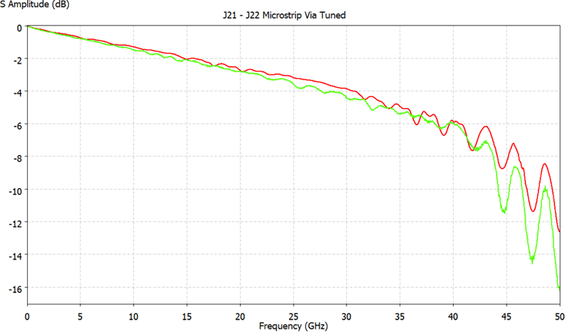
Optimization of an RF launch and general connector design baselines the test vehicle’s core signal integrity. Our engineering teams’ design process focuses on 3D EM optimization suited to the specific design goals of the customer’s project, which is an industry first. Specifically, RF optimization targets differ based on needs of serial link characterization versus de-embedding. WRT designs to a target return loss mask, based on the application. Serial link RF launch optimization goals focus on the power spectral density of the intended data rate and coding, whereas de-embedding needs to have broadband good return loss.

The RF Launch Program
The initial WRT RF connector PCB launch optimization process:
• Meeting to establish signal integrity goals, which can extend to the general test fixture. WRT team provides guidance for Extreme Signal Integrity (ESI).
• Review or create a stackup for materials and ability to optimize to target signal integrity versus frequency.
• Review of the PCB stackup – address potential resonance, Design for Manufacturing Issues, suitability for optimizing to target ESI.
You can read about the entire process here.
WRT has a highly proprietary material ID methodology, using a host of structures that are used to fit material ID in X-Y and Z PCB orientation. There is both a model-based pre-fabrication and measure-based post-verification phase built into each program. Our material Identification and modeling is EDA-centric, fitting the models in 3D electromagnetic (EM) simulation software.
Construction of a reduced size Channel Modeling Platform (CMP) that focuses solely on material ID is core to this activity. There is a partial set of verification structures that are used to verify the models.
In the post-fabrication phase, measurements of the CMP undergo comprehensive S-parameter quality checks which proceeds careful calibration. Cross-sectional analysis using a PCB test strip included with each CMP is also done, as well as PCB fabrication verification.
Measurements, comprehensive model material ID fit reports, PCB libraries of the CMP, and measurement to simulation examples are included in each final report.
The Material Identification program is a an investment in the front end of the project, early in the design state. Our systematic methodology yields scores of benefits.
- Modeling using Ansys HFSS (3D), Cadence Clarity
- 3D X-Y and Z axis Dk, Df
- 3D EM simulation to measurement results of vias, transmission lines
- Simulated-to-Measured Correspondence Program and Report
