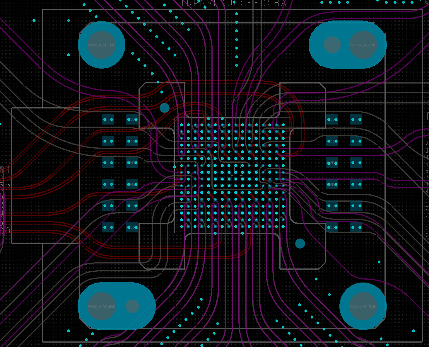
We provide turnkey PCB solutions from library development, schematic creation, layout, and fabrication management. We have supported customers worldwide in many complex designs with critical timelines and lots of technical challenges. We constantly improve our technology capabilities to meet the industry needs with respect to cost, speed, reliability and performance.

Typical Project management by WRT staff includes
- Supervision of and first contact for board design engineer
- Periodic board design checks as sections are completed
- Conduct board placement and post-layout reviews with Customer
- Weekly status reports to Customer
Design Flow
Pre-design Activities
- Identify team, responsibilities
- Set up shared file folder (i.e. Dropbox)
- Review customer design objectives and deliverables (overall function, high-speed design, data rate, max frequency, return loss margins, overall signal integrity)
- Review design timing constraints
- Review initial PCB Placement (Visio mock-up)
- Identification of signal integrity issues
- Risk ID and mitigation strategies, design trade-offs
- Establish schedule, milestones with customer
PCB Design
- Coordinate PCB Symbol Library generation
- Timing constraint set up
- Placement design review w/ customer
- Standard Routing (nets with no timing constraints)
- Balance Routing (nets with timing constraints)
- Critical Design Review
- Post Processing (Create Fab package)
- Deliver Fab Package to fabricator

